Hooking up wiring to 2D semiconductors
Ars Technica » Scientific Method 2014-09-04
As chip manufacturers are getting close to the limits of their ability to scale features down, materials scientists are working hard to provide the raw materials that would let us build circuitry from individual molecules, such as carbon nanotubes. One class of molecules that may find a home in future chips is sheets of material that are a single atom thin.
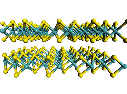
Although graphene, a sheet of carbon atoms, tends to attract the most attention, there are actually a variety of atomically thin materials. And, while graphene is not normally semiconducting, a number of the alternatives are. One of these alternatives, molybdenum disulphide (MoS2), has already been used to create functional electronics. Unfortunately, the performance of these circuits has been erratic. Now, a collaboration of researchers at Rutgers University and Los Alamos National Lab has figured out why: hooking up wires to an atomically thin material is really hard. Fortunately, they've also figured out a solution.
Although MoS2 appears to have what it takes to make great circuitry, early attempts at using it have been inconsistent. As the authors of the new paper note, the mobility values (a measure of how quickly electrons move through the circuit) reported for these circuits can vary by as much as a factor of 400. The problem, the authors suspected, comes from wiring up the circuits. Although it's easy to deposit metal on top of an atomically thin material like MoS2, it's another thing entirely to make sure electrons can easily hop across that junction.
Read 7 remaining paragraphs | Comments