IBM prepares for end of process shrinks with carbon nanotube transistors
Ars Technica » Scientific Method 2012-10-28

The shrinking size of features on modern processors is slowly approaching a limit where the wiring on chips will only be a few atoms across. As this point approaches, both making these features and controlling the flow of current through them becomes a serious challenge, one that bumps up against basic limits of materials.
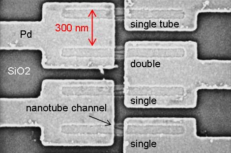
During my visit to IBM's Watson Research Center, it was clear that people in the company are already thinking about what to do when they run into these limits. For at least some of them, the answer would involve a radical departure from traditional chipmaking approaches, switching from traditional semiconductors to carbon nanotubes. And, while I was there, the team was preparing a paper (now released by Nature Nanotechnology) that would report some significant progress: a chip with 10,000 working transistors made from nanotubes, formed at a density that's two orders of magnitude higher than any previously reported effort.
During my visit to Watson, I spoke with George Tulevski, who is working on the nanotube project, and is one of the authors of the recent paper. Tulevski described nanotubes as a radical rethinking of how you build a chip. "Silicon is a solid you carve down," he told Ars, "while nanotubes are something you have to build up." In other words, you can't start with a sheet of nanotubes and etch them until you're left with the wiring you want.
Read 9 remaining paragraphs | Comments