Researchers build a working camera out of atomically thin semiconductors
Ars Technica » Scientific Method 2022-11-18
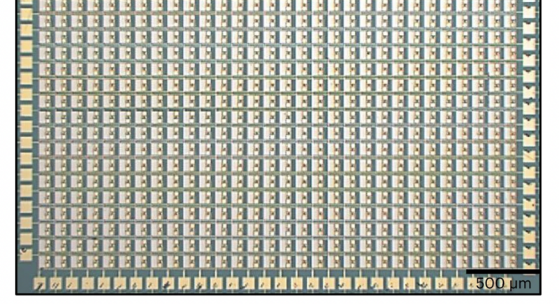
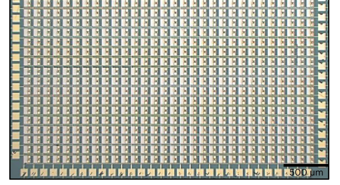
Enlarge / Each one of the silvery squares includes a small sheet of an atomically thin material. (credit: Dodda, et. al.)
Since the isolation of graphene, we've identified a number of materials that form atomically thin sheets. Like graphene, some of these sheets are made of a single element; others form from chemicals where the atomic bonds naturally create a sheet-like structure. Many of these materials have distinct properties. While graphene is an excellent conductor of electricity, a number of others are semiconductors. And it's possible to tune their properties further based on how you arrange the layers of a multi-sheet stack.
Given all those options, it shouldn't surprise anyone that researchers have figured out how to make electronics out of these materials, including flash memory and the smallest transistors ever made, by some measures. Most of these, however, are demonstrations of the ability to make the hardware—they're not integrated into a useful device. But a team of researchers has now demonstrated that it's possible to go beyond simple demonstrations by building a 900-pixel imaging sensor using an atomically thin material.
Making pictures
Most image sensors currently consist of standard silicon semiconductors, manufactured using the usual complementary metal–oxide semiconductor (CMOS) processes. But it's possible to replace the silicon with another semiconductor. In this case, the researchers used molybdenum disulfide, an atomically thin material that has seen a lot of use in experimental devices.